Scanning Electron Microscope: Working, Principle & Parts

SEM stands for Scanning Electron Microscope. In this article, we will throw some light on the principle and working of the scanning electron microscope.
Table of Contents
Introduction
To begin with, the image of the specimen is produced with a focused electron beam that is examined across the area of the specimen. In this, a magnetic lens system targets the beam of electrons into an intense spot on the surface of the specimen. The spot is moved backwards and forward across the specimen by charged plates called beam deflectors. The beam deflector is located between the condenser lens and the specimen. The beam deflectors attract or repel the beam according to signals sent by the deflector circuitry.
Also check out- Difference between SEM and TEM – My Biology Dictionary
As the electron beam sweeps immediately over the specimen molecules in the specimen are excited to a high energy level. Also, emit secondary electrons which are then used to form an image of the specimen surface. Secondary electrons are captured by a detector located rapidly above and to one side of the specimen. In this article, we will throw some light on the principle and working of the scanning electron microscope.

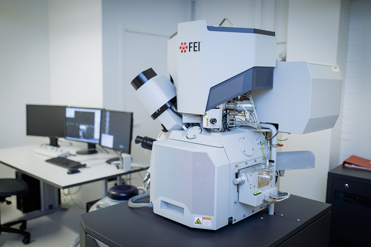
Image source: www.umu.se
Components
The essential component of the detector is the scintillator (a luminescence material that fluoresces when struck by a charged particle or high-energy photon), which when agitated by electrons incident upon it emits photons of light. These photons are used to develop an electronic signal onto the video screen. As the beam travel over the surface of the object electronic deflected to varying degrees. The deflected and emitted electrons are identified by a Photomultiplier tube. Thus it is used to form a 3-D image of the object’s surface features. The resolving power of the SEM is less than that of the TEM (Transmission electron microscopy). After all, since the image formation by SEM is dependent on surface properties it can magnify samples up to many centimetres. It has a greater depth of field. It can thus produce good representative images of the 3D shape of the sample.
History of Scanning Electron Microscope:
An account of the initial history of scanning electron microscopy has been presented by McMullan. Despite this fact, Max Knoll produced a photo with a 50 mm object field width showing channelling contrast by the use of an electron beam scanner. In 1937, it was Manfred von Ardenne who invented the microscope with high resolution by scanning a very small raster with a demagnified and finely focused electron beam. Ardenne applied scanning of the electron beam in an attempt to pass the resolution of the transmission electron microscope (TEM). As well as to reduce substantial problems with chromatic aberration inherent to real imaging in the TEM. He further discussed the different detection modes, possibilities, and theories of SEM, together with the construction of the first high-resolution SEM.
Another work was reported by Zworykin’s group, followed by the Cambridge groups in the 1950s and early 1960s headed by Charles Oatley. All of this finally led to the marketing of the first commercial instrument by Cambridge Scientific Instrument Company as the “Stereoscan” in 1965, which was conveyed to DuPont.
Principle of SEM:
Contrary to the Transmission Electron Microscope which uses transmitted electrons, the scanning electron Microscope particularly uses emitted electrons. SEM works on the principle of applying kinetic energy to produce signals on the interaction of the electrons. Those electrons are secondary electrons, backscattered electrons, and diffracted backscattered electrons. Then these electrons are used to view crystallized elements and photons. Secondary and backscattered electrons are used to form an image. The secondary electrons emitted from the sample play the primary role of detecting the morphology and topography of the specimen. On the other hand, backscattered electrons show a contrast in the composition of the elements of the specimen.
Sample preparation:
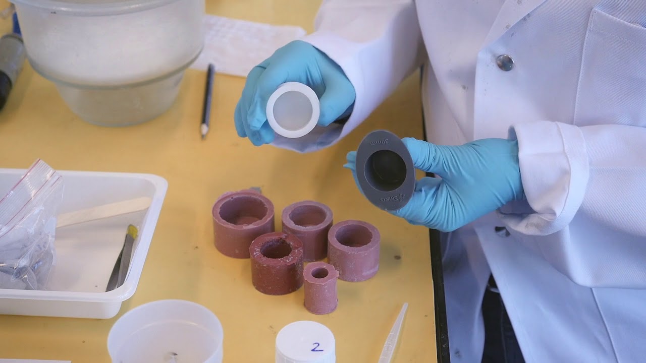
The material is primarily fixed by submerging in 2.8% glutaraldehyde in 0.1M Hepes buffer and pH 7.2 (with 0.02% Triton X-100), for many hours at room temperature or overnight at 4°C. Then the material is washed thrice (each 5 -10 minute duration) in 0.1 M Hepes buffer, pH 7.2. Dehydration is completed for 10 min. in (25% ethanol, 50% ethanol, 70% ethanol, 85% ethanol, and 95% ethanol), 2 x 10 min. in 100% ethanol, and 10 min. in 100% ethanol. It is followed by Critical Point Drying which is an automated process and takes almost 40 minutes to complete. Later the sample is mounted onto a metal stub with double-sided carbon tape. Lastly, sputter Coating is done by applying a thin layer of metals (gold and palladium) over the sample using an automated sputter coater.
Watch here- SEM, Sample preparation – YouTube
Working of Scanning Electron Microscope:
Let’s understand the steps behind working of SEM:
- The source of the electrons and the electromagnetic lenses are from tungsten filament lamps. These are placed at the upper part of the column. It is similar to those of the TEM.
- After thermal energy is applied to the electron source the electrons are emitted. It allowed moving in a rapid motion to the anode, which has a positive charge.
- The beam of electrons interacts with the specimen to generate signals. The signal gives information about the surface topography and composition of the specimen.
- Even air-dried samples can be examined directly, the specimen does not need special treatment for visualization under the SEM.
- The samples are mounted and coated with a delicate layer of heavy metal elements. It allows spatial scattering of electric charges on the surface of the specimen allowing better image production, with high clarity.
- Scanning by this microscope is captured by tapering a beam of electrons back and forth over a thin section of the microscope.
- When the secondary electrons reach and get in the detector, they strike a scintillator. It emits flashes of light which get converted into an electric current by a photomultiplier, sending a signal to the cathode ray tube. Then it produces an image that looks like a television picture that can be viewed and photographed.
- The quantity of secondary electrons that enter the detector is greatly defined by the nature of the specimen i.e raised surfaces receive large quantities of electrons, entering the detector while depressed surfaces have few electrons reaching the surface and hence few electrons enter the detector.
- Therefore lifted surfaces will appear brighter on the screen while depressed surfaces appear darker.
Parts of SEM:
The major parts of the SEM which are important for the working of Scanning electron microscope are:
- Electron Source – This is where electrons are produced under thermal heat at a voltage of 1kV to 40kV. There are mainly three types of electron sources that can be used that is Tungsten filament, Lanthanum hexaboride, and Field emission gun (FEG)
- Lenses – Lenses have many condenser lenses that focus the beam of electrons from the source through the column. By forming a narrow beam of electrons it forms a spot called a spot size.
- Scanning Coil – Scanning coils are particularly used to deflect the beam over the specimen surface.
- Detector – It’s made up of many detectors that can differentiate the secondary electrons, backscattered electrons, and diffracted backscattered electrons.
- The display device
- Power supply
- Vacuum system
To conclude, SEM is an instrument that produces a highly magnified image by using electrons instead of light to form an image. It also has a very higher resolution, so closely spaced specimens can be magnified at much higher levels. These are expensive and large, and must be housed in an area free of any possible electric, magnetic, or vibration interference.
Thanks for reading
Team MBD


