
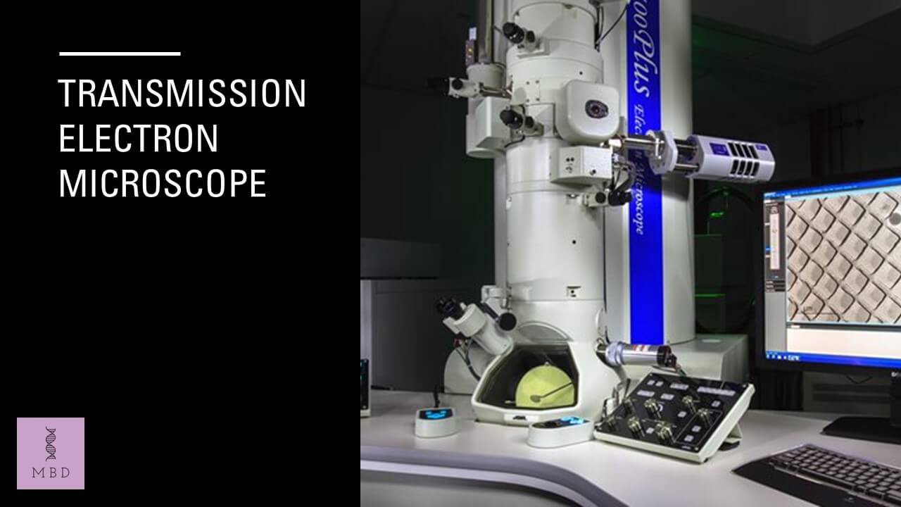
Transmission Electron Microscopy or TEM
Transmission electron microscopy or TEM is a microscopy technique in which a beam of highly focused electrons is directed towards a thin section of the specimen (<200 nm) and allowed to pass through it. Then the electrons either scatter or hit a fluorescent screen at the bottom of the microscope. These microscopes are capable of imaging at a significantly higher resolution than light microscopes. These microscopes enable us to capture the final details of even objects as small as a single column of atoms. It can image thousands of times smaller than a resolvable object seen in a light microscope. In this article, we will learn about the working of a Transmission electron microscope.
Also check out- Scanning Electron Microscope: SEM (Working, Principle, Parts) (mybiologydictionary.com)
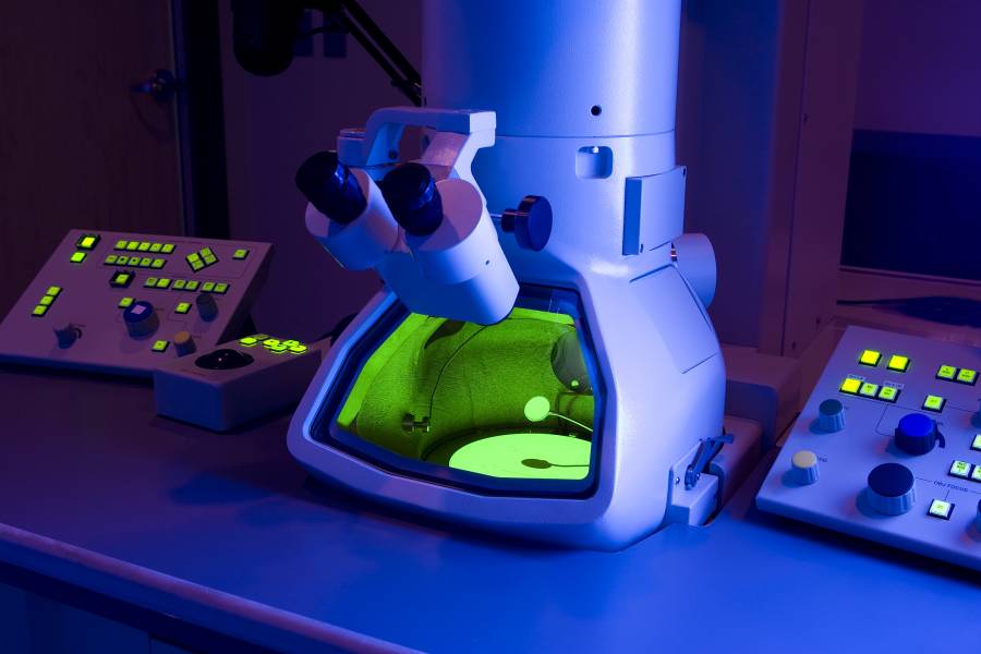
Image source: hub.jhu.edu
Table of Contents
History Behind Transmission Electron Microscopy or TEM
The initial prototype of the microscope was invented by German physicist E. Ruska and the electrical engineer M. Knoll in 1931. This group developed the first TEM with a resolution greater than that of light in 1933. Then came up with the first commercial TEM in 1939. It was first installed in the Physics department of IG Farben Werke. Ruska was later awarded the Nobel Prize in physics for the development of transmission electron microscopy in 1986.
Further with the development of Transmission electron microscopy, the associated technique of Scanning Transmission electron microscopy was introduced. Though it remained underdeveloped till the 1970s. Jannick Meyer and his group described the direct visualization of light atoms such as carbon and even hydrogen atoms using TEM and a clean single-layer graphene substrate in 2008.

Katherine Esau next to her transmission electron microscope. Image source: www.ccber.ucsb.edu
Principle Of Transmission electron microscope (TEM)
- Transmission electron microscopy or TEM works on the principle that electrons possess a wave-like character. The electrons are made to pass through the specimen and the image is formed on the fluorescent screen, either by using the transmitted beam or by using the diffracted beam.
- Electrons are emitted with increased acceleration potential from a heated filament into the vacuum. These will have a small wavelength. They have energy high enough to penetrate several microns distance in solids.
- When these electrons get focused, images with higher resolution are formed.
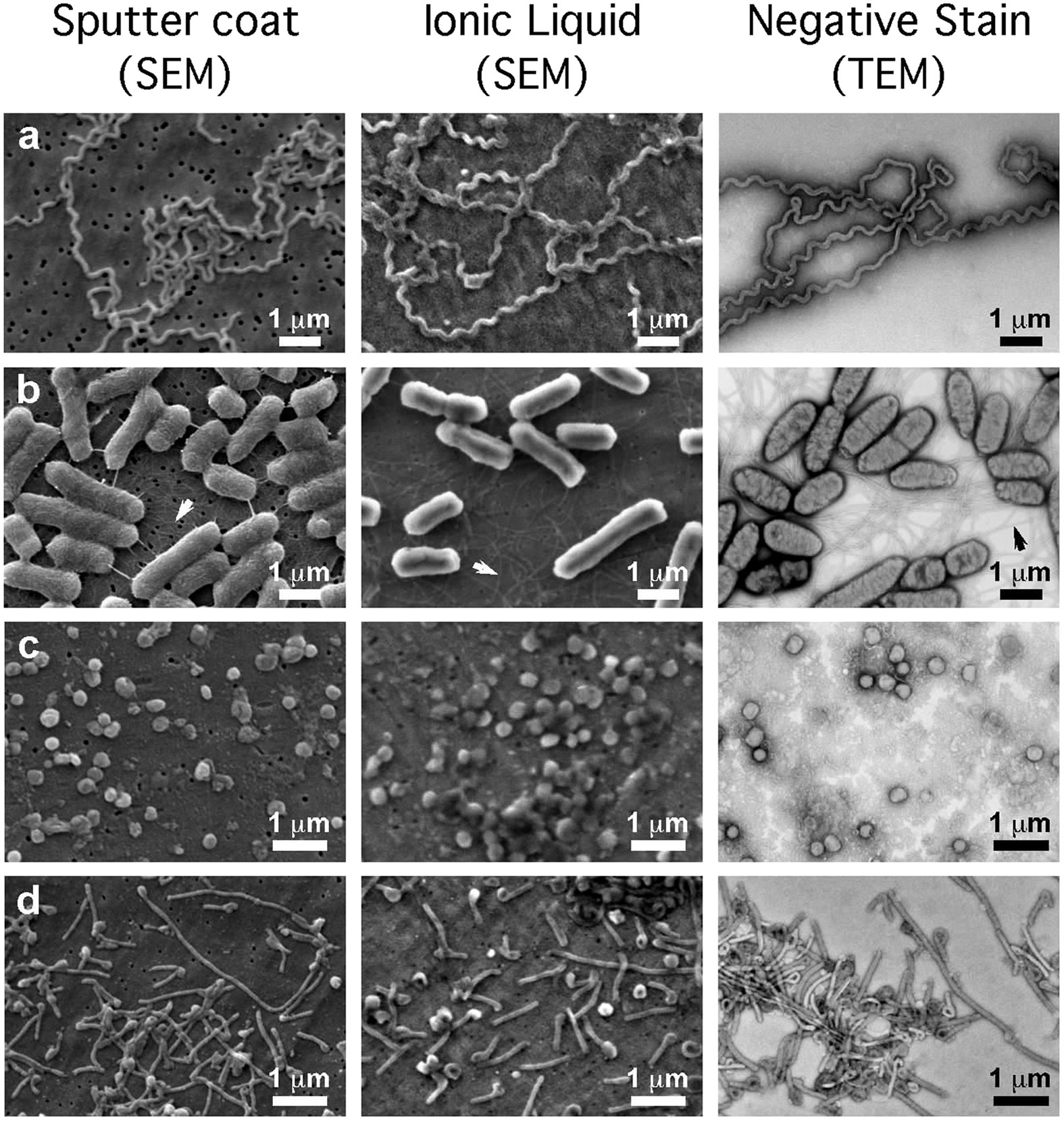
Image source: Golding, C. G., Lamboo, L. L., Beniac, D. R., & Booth, T. F. (2016). The scanning electron microscope in microbiology and diagnosis of infectious disease. Scientific reports, 6(1), 1-8.
Working Of Transmission electron microscope (TEM)
TEM uses a high-voltage electron beam, emitted by an electron gun to create an image. The tungsten filament cathode acts as an electron source in the electron gun. The electron beam then gets accelerated by the anode and is then focused by electrostatic and electromagnetic lenses. This beam then passes through the thin specimen, and the electrons either scatter or hit a fluorescent screen at the bottom of the microscope. Further, the electron beam emerges from the specimen. It carries information about the structure of the specimen that is magnified by the objective lens of the microscope.
Then these transmitted electrons hit the fluorescent screen at the bottom of the microscope. This gives rise to a shadow of the image with its varying parts shown in various darkness according to their density. This image can be then studied directly within the Transmission electron microscope (TEM) or photographed. It is viewed on a fluorescent viewing screen coated with a phosphor or scintillator material.
Components Of Transmission electron microscope (TEM)
VACUUM SYSTEM :
A standard TEM is evacuated to low pressures, typically on the order of 10−4 Pa in order to increase the mean free path of the electron gas interaction. This firstly allows the voltage difference between the cathode and the ground without generating an arc, and secondly to reduce the collision frequency of electrons with gas atoms to negligible levels.
SPECIMEN STAGE :
These are the components of TTEM that allow for the insertion of the specimen holder into the vacuum with minimal loss of vacuum in other areas of the microscope. These specimen holders hold a standard-size sample grid or self-supporting specimen to be viewed. Standard TEM grid sizes are 3.05 mm in diameter, with a thickness and mesh size ranging from a few to 100 μm. The sample is placed on the meshed area having a diameter of approximately 2.5 mm.
ELECTRON GUN :
This itself is formed from the filament, a biasing circuit, a Wehnelt cap, and an extraction anode. Electrons are “pumped” from the filament by connecting the filament to the negative component power supply to the anode plate and the TEM column, thus completing the circuit. The main purpose of it is the divergence of the electron beam to the required angle.
ELECTRON LENS :
The electron lens emulates an optical lens by focusing parallel electrons at some constant focal distance. A majority of them use electromagnetic coils to generate a convex lens. These lenses are made from iron, iron-cobalt, or nickel-cobalt alloys such as permalloy.
APERTURES :
These are the annular metallic components that are actually plate-like and from these, the electrons further than the optical axis may be excluded. The small metallic disc present not only permits axial electrons but also is thick enough to prevent electrons from passing through the disc. In the case of beam-sensitive samples, apertures decrease the beam intensity as electrons are filtered from the beam.

Image source: www.ccber.ucsb.edu
Applications Of Transmission Electron Microscopy or TEM
Transmission electron microscopy or TEM is a major analytical method of microscopy in the physical, chemical, and biological sciences.
1. TEM finds its applications in
- Virology
- Cancer research
- Material science
- Nanotechnology
- Palentology and Palynology
- Life Sciences
2. They are also used in forensic studies and in metallurgy. TEM provides topographical, morphological,
compositional and crystalline information of the specimen.
3. They find wide applications in semiconductor research and analysis and also in the production and manufacture of computer and silicon chips.
4. TEMs are used in technical studies to identify flaws, fractures, and damages to micro-sized objects. Therefore this data can help fix problems and/or help make a more durable, efficient product.
Limitations Of Transmission Electron Microscopy or TEM
There are some drawbacks to using TEM which are as follows.
- It requires laborious sample preparation to produce a sample thin enough to be electron transparent. This makes TEM a relatively time-consuming process with a low throughput of samples.
- TEMs are large and very expensive and their operation and analysis require special training.
- There are chances of the sample structure getting changed during the preparation process.
- There is a potential that the sample may get damaged by the accelerated electron beam, particularly in the case of biological materials.
to conclude, the more recently designed TEM has modifications such that it minimizes the lens aberrations to achieve resolutions below 0.5 Ångströms (50 pm). Th further modifications of TEMs give them the ability to determine the position of atoms within materials widely used in nanotechnology research. Also, the study in semiconductors was made easy due to TEM being another wide application of it. Studies and research is being done to constantly improve the working of Transmission electron microscope. TEM is capable of returning an extraordinary variety of nanometer- and atomic-resolution information. Therefore it is regarded as an essential tool for nanoscience in both biological and materials fields.
Keep reading for more!
Team MBD
Watch here-Working of scanning electron microscope – YouTube


To improve the knowledge about Technical Instruments in biotechnology
To know about different skills